On the Subject of 7400-series

Old school computing, right on your bomb!

  • On this module, you have to work with a 7400-series logic IC. You can find minimalized datasheets for each of these ICs after the first two pages of this manual.
  • To disarm this module, turn on the IC, then set its output pins to the pre-determined state.
  • Next to each of the IC pins you will find an LED. This LED shows the logic state of that pin (high or low), and allows you to toggle it. Caution: Only toggle the state of the input pins according to the datasheet. Touching other pins will result in a strike.
  • There are three special purpose buttons on the right:
    • The top button controls the voltage feeding into the IC. Set the voltage to the correct level within 5 seconds after touching the button, or else the IC will short out and a strike is given.
    • The CLK button connects to the CLK pin of the IC. Pushing this button will send a clock pulse to the IC on the CLK pin. If the IC doesn’t have the CLK pin, pushing this button does nothing.
    • The RST button resets this module to the initial state. You must push this button after you gained a strike, but you can also use it anytime you wish.

Step 1: Determining the voltage

On the IC, the top text indicates the model number. Use the table below and the model number to figure out which voltage to use.

Serial Pattern Voltage Serial Pattern Voltage
74xxx 5 V 74AXCxxx 1.8 V
74HCxxx 3.3 V 74LSxxx 5 V
74AUCxxx 1.1 V 74Cxxx 9 V

Step 2: Determining the disarming logic state

7400-series ICs will have at most 10 logic output pins, which will be clearly marked in the datasheet. Use the table below to get the logic state for disarming the module.

Output pin (if applicable) Output is HIGH (and LOW otherwise) if
0 No parallel port.
1 PS/2 port is present.
2 Lit indicator TRN is present.
3 Lit indicator SIG is NOT present.
4 Serial number of the bomb has a vowel.
5 2 or more batteries.
6 Unlit indicator FRK is present.
7 DVI port is present.
8 Last digit of the bomb’s serial number is odd.
9 Has 1 D battery.

Step 3: Check out the datasheet

This is the last step. Do whatever you can in accordance to the datasheet to get the required logic state.

From the next page is the datasheet of the 7400-series IC. This document is vital for disarming this module, therefore our research department will update it as soon as any new IC types or special information has been found. To keep our printing costs low, we will try to update it in the manner of appending instead of reprinting as much as possible.

This datasheet has been created in collaboration with KTANE Semiconductor for this special purpose only. Public disclosure is prohibited.

7400-series
Introduction

Dear customer,

Thank you for your interest in our products and we hope that you find our 7400-series logic ICs perfect for your needs. To get the most out of your purchase, KTANE Semiconductor presents to you this master datasheet of the 7400-series. In here, you will find all details you need to integrate our ICs into your existing designs.

Before we get into the datasheet, you might find these FAQs helpful:

  • Q: What are the differences between 74595 IC and 74HC595 IC?

    A: The main difference is the operating voltage and logic level voltage. Full details can be found on our website. In this datasheet we will use the 74xxx designation.

  • Q: I noticed there’s a second line of marking on the IC. What do they mean?

    A: The second line of marking indicates when the IC was manufactured. We use YYWWLLLL format. YY is the year, for example 97 for 1997 and 16 for 2016. WW is the week number of that year. LLLL is the internal lot identifier.

  • Q: How do I find out the pin number of the IC?

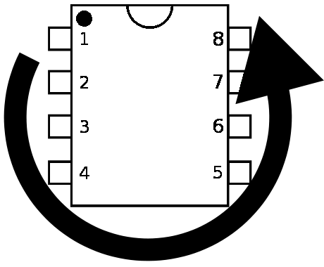
    A: For the Dual In Line (DIP) package: First, locate a small circle on the IC. This circle indicates pin 1. Then, count the pin number anti-clockwise as shown on the right.

  • Q: How does the layout of this datasheet work?

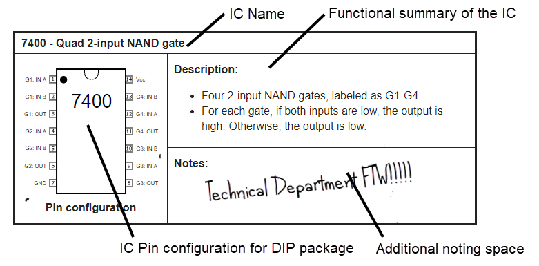
    A: We try to make this datasheet as easy to use as possible with our 4-section design. Refer to the example below:


Page 3
7400-series
7400 - Quad 2-input NAND gate
Pin configuration

Description:

  • Four 2-input NAND gates, labeled as G0-G3
  • For each gate, if both inputs are high, the output is low. Otherwise, the output is high.
Notes:
No additional info
7402 - Quad 2-input NOR gate
Pin configuration

Description:

  • Four 2-input NOR gates, labeled as G0-G3
  • For each gate, if both inputs are low, the output is high. Otherwise, the output is low.
Notes:
If the IC was produced in November of any year, defusing bits are always 1001.
7404 - Hex inverter gate
Pin configuration

Description:

  • Six NOT gates, labeled as G0-G5
  • For each gate, the input will be inverted on the output.
Notes:
Set the 4th bit to 0 if the lot no. is less than 1100.

Page 4
7400-series
7408 - Quad 2-input AND gate
Pin configuration

Description:

  • Four 2-input AND gates, labeled as G0-G3
  • For each gate, if both inputs are high, the output is high. Otherwise, the output is low.
Notes:
The AUC series chips have NAND gates inside.
7410 - Triple 3-input NAND gate
Pin configuration

Description:

  • Three 3-input NAND gates, labeled as G0-G2
  • For each gate, if all inputs are high, the output is low. Otherwise, the output is high.
Notes:
All chips made after 2016 are fakes! G1 is somehow an OR gate.
7411 - Triple 3-input AND gate
Pin configuration

Description:

  • Three 3-input AND gates, labeled as G0-G2
  • For each gate, if all inputs are high, the output is high. Otherwise, the output is low.
Notes:
No additional info.

Page 5
7400-series
7420 - Dual 4-input NAND gate
Pin configuration

Description:

  • Two 4-input NAND gates, labeled as G0-G1
  • For each gate, if all inputs are high, the output is low. Otherwise, the output is high.
Notes:
For some reason, tapping CLK three times with exactly 2 D batteries will defuse the module.
7421 - Dual 4-input AND gate
Pin configuration

Description:

  • Two 4-input AND gates, labeled as G0-G1
  • For each gate, if all inputs are high, the output is high. Otherwise, the output is low.
Notes:
No additional info.
7427 - Triple 3-input NOR gate
Pin configuration

Description:

  • Three 3-input NOR gates, labeled as G0-G2
  • For each gate, if all inputs are low, the output is high. Otherwise, the output is low.
Notes:
No additional info.

Page 6
7400-series
7430 - Single 8-input NAND gate
Pin configuration

Description:

  • One 8-input NAND gate
  • If all inputs are high, the output is low. Otherwise, the output is high.
Notes:
Turn on all NC pins before turning on the power!
7432 - Quad 2-input OR gate
Pin configuration

Description:

  • Four 2-input OR gates, labeled as G0-G3
  • For each gate, if all inputs are low, the output is low. Otherwise, the output is high.
Notes:
No additional info.
7434 - Hex buffer gate
Pin configuration

Description:

  • Six buffer gates, labled as G0-G5
  • For each gate, if the input is high, the output is high. Otherwise, the output is low.
Notes:
Chips made in week no. 10-20 after 2010 are actually hex inverter chips.

Page 7
7400-series
7442 - BCD to decimal decoder
Pin configuration

Description:

  • Input A is the least and D the most significant bit.
  • Converts the input bits to decimal. The output pin with the resulting number is low. All other pins are high.
  • Inputs of 10 or higher will result in all-high output.
Notes:
The output pin that is low = port count.
74138 - 3 to 8 line demultiplexer
Pin configuration

Description:

  • Input A is the least and C the most significant bit.
  • Converts the input bits to decimal. The output pin with the resulting number is low. All other pins will be high.
  • Turn on multiplexing by setting G1 to HIGH and G2A and G2B to LOW, else all output pins will be high.
Notes:
The output pin that is low = battery count.
74192 - Decade up/down counter
Pin configuration

Description:

  • Input A is the least and D the most significant bit.
  • Load initial data into the counter by pulsing low on PL.
  • Count up by setting PL and DOWN to high then pulse UP high, and vice versa.
  • Counting up from 9 will result in rollover, and vice versa.
Notes:
No additional info.

Page 8
7400-series
74160 - Synchronous decade counter
Pin configuration

Description:

  • Input A is the least and D the most significant bit.
  • Load initial data into the counter by pulsing low on PE.
  • Start the counter by turning on the clock and setting CEP and CET to high.
  • The counter will restart from 0 if the chip is reset or if it counts over 9.
Notes:
If the disarming state is over 9 (1001), subtract 9 from it. Stop counting at the correct output to defuse the module.
74161 - Synchronous 4-bit counter
Pin configuration

Description:

  • Input A is the least and D the most significant bit.
  • Load initial data into the counter by pulsing low on PE.
  • Start the counter by turning on the clock and setting CEP and CET to high.
  • The counter will restart from 0 if the chip is reset or if it counts over 15.
Notes:
Stop the counting at correct output to defuse the module. PRESS RESET FIRST AFTER POWER ON!!!!

Page 9
7400-series
74193 - 4-bit up/down counter
Pin configuration

Description:

  • Input A is the least and D the most significant bit.
  • Load initial data into the counter by pulsing low on PL.
  • Count up by setting PL and DOWN to high then pulse UP high, and vice versa.
  • Counting up from 15 will result in rollover, and vice versa.
Notes:
If the IC was made in 1990-1995, you MUST start counting from 8.
74238 - 3 to 8 line non-inverting demultiplexer
Pin configuration

Description:

  • Input A is the least and C the most significant bit.
  • Converts the input bits to decimal. The output pin with the resulting number is high. All other pins will be low.
  • Turn on multiplexing by setting G1 to HIGH and G2A and G2B to LOW, else all output pins will be low.
Notes:
The output pin that is high = lit indicator count.

Page 10